
AIoT Software for Assembly, Packaging, and Testing
Packentra AI delivers enterprise AIoT software for Assembly, Packaging, and Testing with AI, IoT, RFID, BLE, UWB, wafer lot tracking, FOUP tracking, reticle management, cleanroom workforce visibility, WIP control, wafer genealogy, MES integration, SECS/GEM connectivity, and semiconductor manufacturing traceability.
AI-Driven Identification, Location, and Traceability Software for Advanced Assembly, Packaging, and Testing Facilities
Improve cleanroom workforce visibility, semiconductor fab access governance, FOUP and reticle tracking, wafer lot identification, wafer genealogy, work-in-progress management, semiconductor inventory control, and manufacturing traceability using enterprise AI and IoT software designed specifically for advanced Assembly, Packaging, and Testing environments.
Assembly, Packaging, and Testing is among the most sophisticated manufacturing disciplines in the world. A modern 200 mm or 300 mm wafer fabrication facility may process tens of thousands of wafer lots simultaneously through hundreds or even thousands of tightly controlled process operations. Every wafer carrier, Front Opening Unified Pod (FOUP), reticle, process recipe, production asset, operator, maintenance engineer, consumable, and production material must be accurately identified and coordinated while maintaining nanometer-level manufacturing precision.
Unlike discrete manufacturing, Assembly, Packaging, and Testing depends on continuous process synchronization across photolithography, oxidation, diffusion, ion implantation, chemical vapor deposition (CVD), physical vapor deposition (PVD), atomic layer deposition (ALD), plasma etching, chemical mechanical planarization (CMP), wafer cleaning, metrology, inspection, defect review, and electrical wafer sort. Production delays, misplaced FOUPs, unauthorized cleanroom access, missing reticles, inaccurate work-in-progress records, or incomplete wafer genealogy can directly affect cycle time, equipment utilization, yield improvement initiatives, and manufacturing efficiency.
Packentra AI delivers enterprise AIoT software purpose-built for Assembly, Packaging, and Testing. The solution focuses on identification, location, production traceability, workflow coordination, and manufacturing execution support instead of traditional environmental monitoring. By combining AI, Industrial IoT, RFID, Bluetooth® Low Energy (BLE), Ultra-Wideband (UWB), industrial Wi-Fi, barcode technologies, computer vision, Industrial Edge AI, and enterprise software integration, Packentra AI helps semiconductor manufacturers establish a trusted digital representation of manufacturing operations across the entire wafer lifecycle.
The software is engineered for leading-edge logic fabs, memory semiconductor manufacturing, analog IC production, power Assembly, Packaging, and Testing, compound semiconductor manufacturing, MEMS fabrication, silicon photonics production, and mature-node wafer fabs. Rather than replacing established manufacturing systems, Packentra AI complements existing semiconductor operations by connecting personnel, production assets, wafer carriers, reticles, process materials, automated material handling systems (AMHS), overhead hoist transport (OHT), stockers, load ports, equipment front-end modules (EFEMs), and enterprise software into a unified identification and traceability solution.
Overview of AIoT for Assembly, Packaging, and Testing
AI and IoT combines AI with connected industrial devices, identification technologies, enterprise manufacturing software, edge computing, machine learning, computer vision, and industrial communication systems. Within Assembly, Packaging, and Testing, AIoT is most effective when it improves who, what, where, when, and which process questions surrounding every manufacturing activity.
Unlike IoT deployments centered on environmental sensing, Packentra AI focuses on identification and location systems across semiconductor manufacturing workflows. Every cleanroom operator, process engineer, maintenance technician, contractor, FOUP, reticle, wafer lot, wafer cassette, process material, calibration asset, mobile equipment cart, and production tool can be assigned a secure digital identity that remains associated with manufacturing events throughout production. This identification-centric approach enables semiconductor manufacturers to create accurate digital production records while minimizing manual data entry and reducing opportunities for operational errors.
Assembly, Packaging, and Testing presents several operational challenges that make AI and IoT especially valuable:
By integrating AI with trusted identification technologies such as RFID, BLE, UWB, barcode systems, and enterprise identity management, Packentra AI enables fabrication facilities to establish reliable digital traceability throughout production. AI algorithms can then analyze verified manufacturing events to support production planning, asset utilization, workforce coordination, queue management, bottleneck identification, and operational decision-making.
Production managers gain real-time visibility into wafer movement across lithography tracks, deposition tools, etch clusters, ion implantation systems, CMP equipment, metrology stations, inspection tools, and automated storage systems. Engineering teams can rapidly locate delayed wafer lots, identify available reticles, verify authorized personnel access, confirm production routing, and investigate manufacturing exceptions using complete historical records.
Modern semiconductor manufacturers frequently integrate AI and IoT identification solutions with MES, ERP, Advanced Process Control (APC), Fault Detection and Classification (FDC), Equipment Automation Program (EAP), Warehouse Management Systems (WMS), identity management systems, and semiconductor equipment communicating through SECS/GEM and SEMI EDA (Interface A). The result is improved production visibility, stronger operational governance, more reliable wafer genealogy, faster exception handling, enhanced inventory accuracy, reduced manual searching, improved asset utilization, and more efficient semiconductor manufacturing operations.
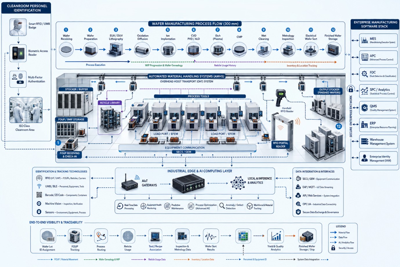
AIoT-Enabled Assembly, Packaging, and Testing Workflow for Intelligent Wafer Manufacturing and Enterprise Traceability
This enterprise workflow diagram illustrates how AIoT software integrates cleanroom personnel, FOUPs, wafer lots, reticles, semiconductor process equipment, AMHS/OHT transport, and enterprise manufacturing systems throughout a modern 300 mm Assembly, Packaging, and Testing facility. It demonstrates end-to-end wafer production, real-time material movement, workforce identification, equipment communication, manufacturing traceability, and AI-driven operational visibility from wafer receiving through finished wafer storage.
Assembly, Packaging, and Testing Applications
Packentra AI is purpose-built for semiconductor wafer fabrication environments where identification, location, manufacturing traceability, and production coordination are mission critical. The software supports both greenfield fabs and mature semiconductor manufacturing facilities across a wide range of device technologies and process nodes.
- Advanced logic Assembly, Packaging, and Testing facilities
- DRAM and NAND memory fabs
- Analog and mixed-signal semiconductor manufacturing
- Power Assembly, Packaging, and Testing
- Silicon carbide (SiC) and gallium nitride (GaN) device production
- MEMS manufacturing facilities
- Silicon photonics fabrication
- RF semiconductor manufacturing
- CMOS image device production
- Research and pilot wafer fabrication facilities
- University semiconductor cleanrooms
- Government semiconductor research laboratories
- Wafer receiving and wafer preparation
- Photolithography and EUV/DUV lithography bays
- Oxidation and diffusion operations
- Ion implantation facilities
- CVD, PVD, and ALD deposition areas
- Plasma etch process bays
- CMP operations
- Wet process and wafer cleaning areas
- Metrology and defect inspection laboratories
- Wafer probe and electrical wafer sort
- Reticle libraries and mask management
- AMHS, OHT, stockers, EFEMs, and fab warehouses
AI Function for AIoT-Enabled Semiconductor Fab Operations
Reliable AI begins with reliable manufacturing data. Packentra AI organizes AI capabilities according to the operational priorities most critical to wafer fabrication: workforce visibility, cleanroom access governance, asset identification, production material management, work-in-progress coordination, and manufacturing traceability.
Modern Assembly, Packaging, and Testing depends on highly trained operators, process engineers, maintenance technicians, equipment specialists, metrology personnel, quality engineers, and contractors working across multiple cleanroom classifications and production shifts.
AI-assisted analytics include:- Wafer Fab Operator Analytics
- Cleanroom Technician Analytics
- Fab Shift Workforce Analytics
- Semiconductor Lone Worker Analytics
- Fab Personnel Flow Analytics
Semiconductor fabs contain highly controlled production zones housing advanced lithography scanners, ion implantation systems, deposition chambers, etch clusters, reticle storage, and proprietary manufacturing technologies.
Packentra AI strengthens access governance through:- Cleanroom Entry Compliance
- Process Bay Access Analytics
- Semiconductor Tool Authorization
- Fab Visitor Access Governance
- Fab Identity Verification
Thousands of production assets circulate continuously throughout a semiconductor fab. FOUPs, reticles, portable metrology equipment, calibration tools, maintenance carts, and mobile cleanroom equipment must remain readily identifiable.
Comprehensive visibility through:- FOUP Location Analytics
- Reticle Tracking Analytics
- Wafer Carrier Analytics
- Semiconductor Tool Utilization
- Fab Mobile Equipment Analytics
IoT Software for AIoT-Enabled Semiconductor Fab Operations
Packentra AI delivers enterprise AI and IoT software specifically engineered for Assembly, Packaging, and Testing. The modular software design allows semiconductor manufacturers to deploy capabilities incrementally while integrating with existing MES, ERP, warehouse management systems, identity management solutions, APC, FDC, EAP, SECS/GEM communications, and enterprise reporting applications.
Assembly, Packaging, and Testing facilities require continuous visibility of authorized personnel working inside highly controlled cleanroom environments. Workforce identification ensures personnel authorization aligns with production activities, equipment qualifications, maintenance schedules, and cleanroom operating procedures.
Software includes:- Cleanroom Badge Management
- Fab Personnel Location Software
- Contractor Access Software
- Fab Shift Attendance
- Cleanroom Muster Software
FOUPs, reticles, SMIF pods, wafer carriers, qualification standards, calibration instruments, portable metrology tools, maintenance equipment, and mobile cleanroom carts represent critical manufacturing resources whose location directly affects production efficiency.
Comprehensive identification through:- FOUP Tracking Software
- Reticle Tracking Software
- Semiconductor Tool Tracking
- Fab Equipment Tracking
- Calibration Asset Software
Assembly, Packaging, and Testing consumes a broad range of controlled materials, including specialty chemicals, photoresists, slurry, process gases, cleanroom garments, filters, spare parts, wafer carriers, quartzware, ceramic components, and maintenance consumables.
Software supporting:- Process Chemical Inventory
- Fab Spare Parts Software
- Cleanroom Consumables Tracking
- Fab Material Replenishment
- Semiconductor Warehouse Tracking
Wafer fabrication is fundamentally driven by complete production traceability. Every manufacturing operation contributes to wafer genealogy, process history, engineering analysis, yield management, and customer quality requirements.
Comprehensive tracking through:- Wafer Lot Tracking Software
- Fab WIP Tracking
- Semiconductor Traceability Software
- Material Transfer Tracking
- Process Route Tracking
IoT Hardware Technologies for AIoT-Enabled Assembly, Packaging, and Testing
Reliable AI begins with reliable identification hardware. Packentra AI supports identification technologies commonly deployed throughout modern wafer fabrication facilities, enabling organizations to build scalable AI and IoT solutions using proven industrial hardware capable of operating within ISO Class cleanroom environments.
Identification devices establish secure digital identities for wafer lots, FOUPs, reticles, personnel, production assets, and manufacturing materials.
Supported hardware includes:- Cleanroom RFID Readers
- Semiconductor RFID Tags
- Fab BLE Beacons
- BLE Industrial Gateways
- Wafer Barcode Scanners
Personnel identification technologies help semiconductor manufacturers enforce access authorization while maintaining complete digital records of workforce movement.
Typical devices include:- Cleanroom Smart ID Badges
- Biometric Access Readers
- UWB Personnel Wearables
- RFID Employee Cards
- Fab Access Terminals
High-value production assets require durable identification capable of surviving repeated manufacturing cycles and continuous cleanroom operation.
Supported hardware:- FOUP RFID Tags
- Reticle RFID Tags
- Fab Handheld RFID Readers
- RFID Portal Readers
- BLE Equipment Tags
Enterprise AIoT solutions require secure communication between identification devices, manufacturing software, edge computing resources, and semiconductor production equipment.
Supported connectivity:- AI and RFID for Assembly, Packaging, and Testing
- AI and BLE for Semiconductor Manufacturing
- AI and Industrial Wi-Fi for Wafer Fabs
- AI and LoRaWAN for Fab Logistics
Assembly, Packaging, and Testing facilities generate enormous volumes of operational information that benefit from localized processing close to manufacturing operations.
Deployment using:- Industrial Edge Computers
- AI Edge Gateways
- Machine Vision Computers
- Embedded AI Controllers
- Fab Edge Servers
Integration for Semiconductor Fab Operations
Advanced Assembly, Packaging, and Testing facilities operate through tightly coordinated communication among MES, ERP, AMHS, OHT, semiconductor process equipment, warehouse systems, quality systems, engineering applications, and enterprise identity management. Packentra AI is designed to integrate with these existing manufacturing systems, enabling organizations to enhance identification, location, and traceability without disrupting validated production workflows.
Enterprise integration allows identification and location information to become part of broader semiconductor manufacturing processes.
Supported integration capabilities:- Fab MES Integration
- Semiconductor ERP Integration
- Manufacturing Data Exchange
- Fab Production Synchronization
- Enterprise Identity Management Integration
Semiconductor manufacturing equipment continuously generates operational events that become significantly more valuable when linked with trusted identification information.
Connectivity through:- SECS/GEM Integration
- SEMI Equipment Integration
- Equipment Automation Program (EAP) Connectivity
- Tool Communication Services
- Edge Device Connectivity
Modern semiconductor organizations depend on secure information exchange across engineering, manufacturing, logistics, maintenance, quality assurance, and enterprise business systems.
Packentra AI supports:- Manufacturing API Integration
- Production Event Streaming
- Fab Data Synchronization
- Manufacturing Master Data Management
- Enterprise Messaging Services
Every semiconductor manufacturer has unique cybersecurity requirements, operational policies, and infrastructure strategies. Packentra AI supports multiple deployment models:
Drawing upon experience developed within Aperture Venture Studio and supported by GAO, Packentra AI benefits from more than two decades of industrial IoT expertise, thousands of customer engagements, extensive research and development investments, rigorous quality assurance, and technical leadership provided by Ph.D. engineers and experienced industrial specialists. This practical experience has supported projects involving Fortune 500 manufacturers, leading research institutions, universities, and government agencies throughout North America.
Benefits of AIoT for Assembly, Packaging, and Testing
Successful AI and IoT initiatives within Assembly, Packaging, and Testing improve operational decision-making by establishing reliable identification and traceability throughout manufacturing rather than simply collecting more operational data.
- Improved wafer lot visibility throughout complex manufacturing routes
- Faster FOUP identification and location
- More efficient reticle management
- Better utilization of portable production assets
- Improved cleanroom workforce accountability
- Stronger cleanroom access governance
- Enhanced work-in-progress visibility
- More accurate semiconductor inventory management
- Improved spare parts availability
- Reduced manual searches for manufacturing assets
- Better wafer genealogy supporting yield engineering
- Faster production bottleneck identification
- Improved production dispatching and queue management
- Reduced manufacturing cycle time variability
- More reliable production history records
- Improved engineering root cause investigations
- Better synchronization with Manufacturing Execution Systems
- Increased operational consistency across multiple fabs
Trusted Digital Traceability
Because production events remain associated with verified digital identities, engineering organizations gain more dependable historical information for yield improvement, process qualification, equipment optimization, preventive maintenance, and continuous manufacturing improvement.
Why Packentra AI
Packentra AI is dedicated to enterprise AI and IoT software for Assembly, Packaging, and Testing, with an emphasis on identification, location, manufacturing traceability, and production coordination. Every capability is designed around the operational realities of modern wafer fabs.
The software is built specifically for semiconductor wafer fabrication using terminology, workflows, and operational practices familiar to semiconductor manufacturers. Native support for FOUP management, reticle identification, wafer genealogy, WIP coordination, semiconductor inventory management, cleanroom access governance, and semiconductor equipment connectivity ensures strong alignment with fab operations.
AI performs best when built upon trusted operational information. Packentra AI prioritizes accurate identification of personnel, wafer lots, FOUPs, reticles, production materials, and manufacturing assets before applying machine learning, operational analytics, and workflow optimization. This approach improves data quality while reducing inconsistencies introduced by manual processes.
Rather than replacing existing manufacturing systems, Packentra AI extends their capabilities by integrating with MES, ERP, SECS/GEM communications, SEMI EDA (Interface A), warehouse systems, quality applications, and enterprise identity management. Manufacturers preserve existing investments while improving operational visibility.
Packentra AI supports deployment in cloud, on-premises, hybrid, industrial edge, and multi-fab environments. Built within Aperture Venture Studio with support from GAO, Packentra AI leverages decades of industrial IoT experience, continuous R&D investment, comprehensive quality assurance, and leadership from Ph.D. professionals. This experience includes projects supporting Fortune 500 companies, leading research organizations, prestigious universities, and government agencies throughout the United States and Canada.